Samsung and SK hynix sign $950 billion in AI chip deals with US big tech

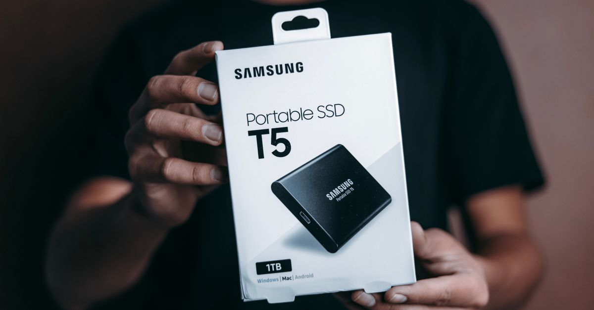
Samsung Electronics and SK hynix have signed AI chip and infrastructure partnerships worth a combined $950 billion (approximately 1,390 trillion won) with global technology firms including Broadcom, Nvidia, and Microsoft, according to Seoul Economic Daily reporting dated July 27, 2026. The agreements convert previously annual memory supply contracts into long-term agreements (LTAs) of five years or more, positioning the two Korean suppliers as central partners in AI infrastructure.
Samsung Electronics signed a business agreement with Broadcom worth $200 billion through 2030, covering 2-nanometer foundry production and advanced packaging. SK hynix secured roughly $750 billion in contracts, including a five-year long-term memory supply deal with Nvidia and an AI server memory supply partnership with Microsoft. Jun Young-hyun, head of Samsung's Device Solutions Division, said tightly integrated memory, logic, and advanced packaging solutions are the company's "core competitive edge."
SK Group separately unveils $500 billion AI alliance with NVIDIA, Microsoft, and Anthropic
At the K-AI Summit in San Francisco on July 24 (local time), SK Group Chairman Chey Tae-won announced a separate AI infrastructure partnership valued at more than $500 billion with NVIDIA, Microsoft, Anthropic, and AWS, Business Korea reported on July 27. The plan includes a 2-gigawatt AI factory to be built by SK Telecom using next-generation NVIDIA GPUs and SK hynix HBM4 memory, with phased operations beginning in 2027.
The NVIDIA partnership spans AI factories and memory supply, while SK hynix extended its cooperation with Microsoft on long-term server memory solutions. SK Telecom also signed an agreement with Anthropic for a gigawatt-class data center in South Korea and with AWS to expand AI computing capacity. Chey framed the alliance as positioning South Korea as an AI infrastructure hub connecting the United States, Europe, and Asia.
CXMT soars on Shanghai debut, becoming China's most valuable company
ChangXin Memory Technologies (CXMT) rose as much as 530 percent on its Shanghai trading debut on July 27, lifting its market capitalization to 3.65 trillion yuan (about US$540 billion) and surpassing Industrial and Commercial Bank of China as mainland China's most valuable company, Channel News Asia reported. The rise underscored how AI-related memory demand is reshaping valuations across the sector.
The IPO raised 66.6 billion yuan (US$9.8 billion) in China's biggest mainland tech share sale, beating the 46.3 billion yuan raised by Semiconductor Manufacturing International Corp in 2020, according to Bloomberg News figures cited by CNA. Crypto Briefing separately reported the offering was priced at 57.9 billion yuan ($8.55 billion), making it the largest mainland China listing since Agricultural Bank of China in 2010. CXMT is the world's fourth-largest DRAM maker; CNA estimated its market share at around 8 percent, while Crypto Briefing cited roughly 7.7 percent as of 2025. Apple is reportedly testing CXMT's DRAM chips, though TrendForce analyst Ellie Wang noted the IPO is unlikely to ease the current shortage immediately because new capacity typically takes a year or longer to come online.
Samsung outlines 2-nanometer HBM5 base die, targeting more than 50 percent speed gain
Samsung Electronics will apply a Gate-All-Around-based 2-nanometer foundry process to the base die of its next-generation HBM5 memory, with operating speed targeted at more than 50 percent above the current HBM4E, EDAILY reported on July 27. Koo Ja-heum, head of technology development at Samsung's Foundry Business Division, said higher-density through-silicon vias will accompany the process shift.
Samsung previously used its fourth-generation 4-nanometer process for the base dies of HBM4, which entered mass production in February, and for 12-layer HBM4E samples supplied in May. The HBM4E base die reaches operating speeds above 14 gigabits per second, with power savings and improved heat dissipation achieved through metal-layer placement. Samsung said the HBM4 base die met performance and yield targets from its first sample, citing a company-wide task force.
Siemens and NVIDIA expand partnership for self-verifying AI agents in chip design
Siemens and NVIDIA announced an expansion of their partnership to bring self-verifying agentic AI workflows to electronic design automation, according to a July 27 Siemens release and GamesBeat coverage. Updates to Siemens' Fuse EDA AI Agent integrate NVIDIA's NeMo Gym open library, OpenShell secure runtime, Nemotron models, Switchyard reasoning, and CUDA-X libraries to help semiconductor and printed circuit board engineering teams validate AI-driven decisions against physics-based EDA engines.
Siemens EDA chief AI strategy officer Amit Gupta said the collaboration aims to deliver "trusted, self-verifying AI workflows" that improve result quality, time-to-results, and tool-calling reliability across long-running engineering workloads. NVIDIA's Timothy Costa said the combination targets semiconductor and PCB design, among "the most complex engineering challenges in the world." The Fuse EDA AI Agent is now integrated into Siemens' Intelligence Center X enterprise industrial AI environment.
Follow-up signals
SK Telecom's 2-gigawatt AI factory is scheduled to begin phased operations in 2027. TrendForce noted CXMT's capacity expansions will take roughly a year or more to materially ease the global DRAM shortage, while Samsung's HBM5 mass production timeline was not specified in the available reporting. Siemens did not provide a release date for the broader Fuse-NVIDIA integration beyond availability within Intelligence Center X.
Share this article