Reported A14 production schedule

TSMC is reportedly preparing to begin mass production of its A14 semiconductor process node in the first half of 2028, according to coverage published on October 29. The schedule follows risk production planned for the second half of 2027. The reviewed material did not include a TSMC announcement confirming the reported timeline.
The production process is separate from a research result disclosed by TSMC for A14 SRAM. The company’s research abstract described a cell area below 0.017 square micrometers, while mass production remained planned for 2028.
A14 SRAM research result
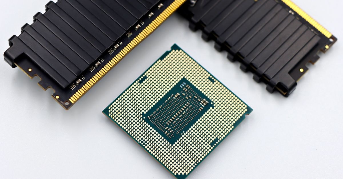
TSMC disclosed in a research abstract that its A14 technology can shrink an SRAM cell to below 0.017 square micrometers. SRAM serves as cache memory in logic chips such as CPUs and GPUs, and cell area measures the physical area of the circuit that stores one bit.
The abstract is a research result, not a production specification. TSMC’s earlier research included a 0.0199-square-micrometer SRAM cell for 3nm in 2022 and a 0.021-square-micrometer high-density bit cell introduced with N2 research in 2025. Those results involved different designs and were not measured under identical conditions.
What remains to be verified
The next documented milestone is TSMC’s planned presentation of the A14 work at the International Electron Devices Meeting on December 14. Whether the reported mass-production schedule and the broader capacity plans are implemented will require confirmation beyond the research abstract and secondary reporting reviewed here.
Share this article